
|
Aqua PCIe Lanes: CPU vs PCH Distribution |
Post Reply 
|
| Author | |
rangulicon 
Newbie 
Joined: 28 Nov 2019 Status: Offline Points: 16 |
 Post Options Post Options
") Thanks(0) Thanks(0)
 Quote Reply Quote Reply
 Topic: Aqua PCIe Lanes: CPU vs PCH Distribution Topic: Aqua PCIe Lanes: CPU vs PCH DistributionPosted: 28 Nov 2019 at 1:04pm |
|
Can anyone help in providing a full breakdown of how PCIe lanes for CPU and PCH are distributed among all slots and devices on the Aqua motherboard?
It'd also be great to know how populating certain slots affects available lanes for other devices. The motherboard manual is not very helpful at describing any of this in detail for anything but the main PCIe slots. If we can compile this information here it will help other Aqua motherboard owners in the future. |
|
 |
|
|
Ray62
Groupie 

Joined: 01 Jul 2018 Location: Germany, Berlin Status: Offline Points: 706 |
Post Options
Thanks(1)
Quote Reply
Posted: 29 Nov 2019 at 6:29am |
|
First, the X570 Aqua and the X570 Creator are the same (without regarding the cooling).
As in nearly all X570 boards: CPU: PCIE1 PCIe 4.0 x16 with 16 lanes (8 lanes, if PCIE4 is used too) PCIE4 PCIe 4.0 x16 with 8 lanes First M2 slot with PCIe 4.0 4x PCH: PCIE6 PCIe 4.0 x16 with 4 lanes Second M2 slot with PCIe 4.0 4x 4 SATA ports Aqua/Creator specific: * Via PCH->PCIe 2.0 Controller->HUB, the following connections share bandwidth via one PCIe 2.0 lane: PCIE2 PCIe 2.0 x1 PCIE3 PCIe 2.0 x1 PCIE5 PCIe 2.0 x1 4 SATA ports All the other devices (USB, WiFi, NET, Audio) not regarded here. * This info is from here: https://www.tomshardware.com/reviews/asrock-x570-creator-motherboard |
|
|
Asrock Fatal1ty X370 Professional Gaming Offline
Under test: MSI X570_MEG_ACE | AMD Ryzen 9 3900X | Scythe Mugen5 | 2x16GB F4-3200C14D-32GTZ@3466 | ASUS GeForce GTX 1080 Ti FE |
|
|
|
|
rangulicon
Newbie
Joined: 28 Nov 2019 Status: Offline Points: 16 |
Post Options
Thanks(0)
Quote Reply
Posted: 30 Nov 2019 at 4:19am |
|
Thank you for the info @Ray62.
I've seen people report that other X570 based boards split multiple M.2 slots between CPU and PCH based lanes. It great to have confirmation that for the Creator and Aqua both M.2 slots are on the CPU based PCIe Lanes. |
|
|
|
|
Ray62
Groupie
Joined: 01 Jul 2018 Location: Germany, Berlin Status: Offline Points: 706 |
Post Options
Thanks(0)
Quote Reply
Posted: 30 Nov 2019 at 4:43am |
What confirmation??? PCH: PCIE6 PCIe 4.0 x16 with 4 lanes Second M2 slot with PCIe 4.0 4x 4 SATA ports 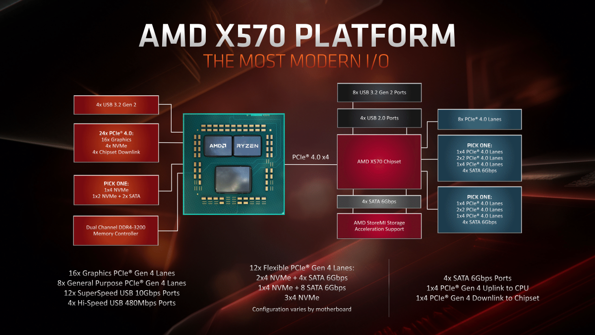
|
|
|
Asrock Fatal1ty X370 Professional Gaming Offline
Under test: MSI X570_MEG_ACE | AMD Ryzen 9 3900X | Scythe Mugen5 | 2x16GB F4-3200C14D-32GTZ@3466 | ASUS GeForce GTX 1080 Ti FE |
|
|
|
|
rangulicon
Newbie
Joined: 28 Nov 2019 Status: Offline Points: 16 |
Post Options
Thanks(0)
Quote Reply
Posted: 30 Nov 2019 at 7:43am |
|
Apologies I misread what you wrote. So all x570 boards split the M.2 between CPU and PCH. Good to know.
|
|
|
|
|
rangulicon
Newbie
Joined: 28 Nov 2019 Status: Offline Points: 16 |
Post Options
Thanks(0)
Quote Reply
Posted: 20 Dec 2019 at 3:11am |
|
Here is a Block Diagram I find gives the most info regarding how connections are distributed between the chipset and CPU PCIe lanes.

|
|
|
|
|
Ray62
Groupie
Joined: 01 Jul 2018 Location: Germany, Berlin Status: Offline Points: 706 |
Post Options
Thanks(0)
Quote Reply
Posted: 20 Dec 2019 at 5:14am |
|
It would be nice to see those diagrams in all Asrock (and other vendors) mainboard manuals.
I just wonder from which side this image (just an imgur link) is stolen...  And i got it: An new Aqua review @Anandtech: https://www.anandtech.com/show/14951/the-asrock-x570-aqua-motherboard-review- But sad like for all Aqua-Reviews, they also did not test it with a 3950X or at least with a 3900X for showing the real cooling muscles of this board. Isn't it allowed by Asrock? 
|
|
|
Asrock Fatal1ty X370 Professional Gaming Offline
Under test: MSI X570_MEG_ACE | AMD Ryzen 9 3900X | Scythe Mugen5 | 2x16GB F4-3200C14D-32GTZ@3466 | ASUS GeForce GTX 1080 Ti FE |
|
|
|
|
Post Reply
|
|
 Tweet
Tweet
|
| Forum Jump | Forum Permissions You cannot post new topics in this forum You cannot reply to topics in this forum You cannot delete your posts in this forum You cannot edit your posts in this forum You cannot create polls in this forum You cannot vote in polls in this forum |


 Topic Options
 rangulicon wrote: